Analyze
Luminescence studies are central to an extensive range of disciplines, both as a primary experiment and in a minor role for additional discrimination between samples. The sensitivity of luminescence measurements is ideal for studies of the electronic structure of solids, crystalline defects, and impurities. These measurements identify and separate properties of the intrinsic lattice (and defects), contaminants, dopants (trace elements), or secondary inclusions with detection limits frequently well below parts per million. When a high spectral resolution is applied, one can further identify more subtle changes, including stress, location of an ion within the unit cell, or the charge state of impurity.
While the high sensitivity to the local environment is a significant strength of luminescence techniques, a direct consequence is that there is a wide range of mechanisms that can lead to contrast in a cathodoluminescence (CL) map or a peak in a luminescence spectrum. In the following sections, we provide an introduction to interpreting CL data based on the sample type and methods available.
Origins of Contrast
Cathodoluminescence (CL) maps often provide distinctly different information to other signals in the electron microscope. Many other signals are formed as a result of directly observable physical features such as sample size, shape, and topography. However, the information gathered from the CL signal is related to the local optical and electronic properties, and the correct interpretation often requires some careful consideration.
Insulators Semiconductors Metals
You can separate solid materials into three distinct groups based on their electronic structure: Metals, semiconductors, and insulators. Every solid has its characteristic energy-band structure and, the variation in band structure is responsible for the wide range of electrical and optical characteristics observed. In a CL experiment, the luminescence that we measure is a direct result of the interaction of the high energy electron of our electron beam and the sample’s electronic structure. Thus, measurements are sensitive to changes in the electronic structure including a change in the energy of the crystal’s bandgap (composition, stress, temperature), electronic levels within the bandgap (e.g., intentional or unintentional doping/impurities, crystal defects, charge state).

Semiconductors and insulators are characterized by a bandgap—the (energy) distance between the valence band of electrons (electrons bound to an atom or ion in the crystal) and the conduction band (where electrons are free to move within the crystal). The bandgap is a range of energy states that an electron is forbidden to occupy, and energy equal to or greater than the bandgap energy must be provided to excite a valence electron into the conduction band. A semiconductor is a material with an intermediate-sized bandgap whereas a material with a large bandgap is an insulator. In conductors, the valence and conduction bands overlap, and electrons are free to wander the crystal enabling metals to conduct electricity efficiently.
Insulators
Let us first examine the case of CL from insulators such as rocks, minerals, gems, and other dielectric materials. The electron beam imparts energy to the crystal of the sample and can promote an electron from the valence band to the conduction band. However, this energetic state is unstable, and the crystal returns to the ground state by the electron falling from the conduction band to the valence band. The excess energy transforms into heat (phonons), and light (photons) with the energy release of the photon corresponds to the size of the energy transition.

Nevertheless, the energy gap of insulators is too large to produce photons at visible wavelengths (\(Energy ∝ 1/Wavelength\)). Instead, CL at visible, ultraviolet, and infrared wavelengths (180 – 2300 nm) is produced via activators—transition metal ions, rare earth ions, or crystal defects—which place energy levels within the bandgap. The energy (wavelength/color) of the emitted photon relates to the energy transition(s) and, therefore, activator species in a crystal. CL mapping and spectroscopy can reveal the presence and distribution of activators and identify the activator species making it a powerful tool for microanalysis of geological minerals.

An example of a color CL map is shown here. The map differentiates minerals and reveals the distribution of trace elements within individual grains at concentrations as low as 1 – 10 parts per million, making CL an effective tool to reconstruct geological processes based on crystal chemistry. For more information on how to use CL maps for microanalysis, please refer to the Rocks, Minerals, and Gems section.
Semiconductors
A semiconductor’s useful properties are governed by its electronic structure and bandgap. Scientists and engineers strive to understand and control these properties to create more efficient devices or devices with novel properties like transistors, lasers, light-emitting diodes, and solar cells. Semiconductor materials have a narrower bandgap than insulators (0.5 – 6.0 eV typically) and, in these materials, the relaxation of an electron from the conduction band to the valence band (termed band-to-band recombination) often emits a photon with a wavelength that may be termed cathodoluminescence. Thus, CL can be used to determine the bandgap of material (often) with nanoscale spatial resolution. In the example below, a CL spectrum reveals the bandgap of a CdTeS solar cell enabling the alloy composition to be mapped with high precision.

In semiconductors, many crystal defects introduce deep levels into the bandgap. Unlike activators in insulators, energy transitions that take place via deep levels do not release a photon. The band-to-band and deep level recombination pathways are competitive, thus when a semiconductor crystal contains defects (that introduce a deep level) the probability of photon emission is reduced and, in a CL map, can be revealed as areas of dark contrast. In the example shown here, threading dislocations in a semiconductor film are observed where they intersect the surface of a GaN film.

Revealing the electronic structure of defects at cryogenic temperatures
Non-radiative recombination via deep levels requires phonon participation. At cryogenic temperatures, the phonon population can be reduced to such an extent that radiative recombination via the defect levels becomes probable. Cryogenic SEM stages are often used with CL detectors to allow the electronic structure of crystal defects to be determined.
Metals
Metals do not have an electronic bandgap yet still can emit light in a CL experiment; however, the mechanism for light emission is quite different from the cases of semiconductors and insulators discussed previously.
Metals are characterized by having free electrons in the conduction band. It is these free electrons that govern their optical and electronic properties; the sea of free electrons moves through the crystal in response to an electric field to conduct electricity and also controls their optical properties. The electric field of visible light oscillates extremely rapidly and can cause the free electrons near the metal’s surface to oscillate in response. Under the right conditions, the light wave can excite a longitudinal wave of electrons known as a surface plasmon. Not all metals can support surface plasmons, and typically, they exist only over a narrow frequency (wavelength) range however, the surface plasmon has some potentially fascinating advantages:
- Field enhancement—The electric field is extremely localized and results in plasmonic field amplitudes that can be two orders of magnitude larger than the electric field that excited the plasmon; the plasmonic metal behaves like an antenna.
- Long-range propagation—Typically, light does not penetrate very far into a metal (only a few nanometers). However, surface plasmons can travel up to a millimeter along the surface of a metal, thereby opening the possibility for integrated optical and electronic circuits.
- Short wavelength—A surface plasmon has a shorter wavelength than the light of the same frequency does; implying that surface plasmons can be used to focus light below Abbe’s optical diffraction limit.
There has been much interest in metallic nanostructures as the surface plasmons may be controlled by a nanostructure’s size, shape, and composition. In particles smaller than the propagation length of the surface plasmon, surface plasmon resonances may be established with control over the resonant frequencies providing a toolbox for developers of nanophotonics devices. Revealing plasmon resonance modes is critical but presents a significant experimental challenge given the sub-diffraction limit particle size and low luminosity.
Energetic electrons can also be used to generate surface plasmons, and in the electron microscope, we can use CL to analyze surface plasmon behavior as light absorption and emission are reciprocal processes. Furthermore, we can directly correlate the physical structure to the optical properties.
The figure below shows an individual AuPd nanostar, ~100 nm tip-to-tip. The CL map reveals four bright spots, each located at the tip of an arm of the nanostar with strong emission at a wavelength of 600 nm. These hot spots in the CL image correspond to maxima in the local density of optical states in the nanoparticle occurring at the resonance nodes at the nanostar tips. The differing emission polarization at the nodes suggests that the most intense plasmonic modes are dipolar and resonant at opposing tips.

The ability to interrogate the interaction of light and matter far below diffraction limit with wavelength (energy), polarization and angle (momentum) resolution makes CL an ideal technique for nanophotonics studies. For more information, please refer to the Nanophotonics section.
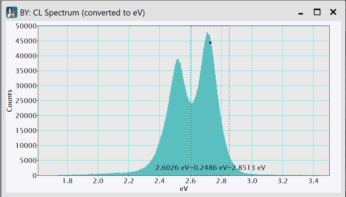
Analyzing Luminescence Spectra
A key method for investigating samples is wavelength spectroscopy. Light is dispersed by wavelength (energy or color) using an optical spectrometer or spectrograph, and the resulting data set is a one-dimensional plot of intensity versus wavelength. Luminescence spectra are typically a series of lines or peaks of finite width on a zero-level background. The peak shape, central wavelength, and full width half maximum (FWHM) are essential characteristics that assist in identifying the mechanism responsible for the luminescence. However, it is often difficult to unambiguously assign the species responsible without other information.
In atomic emission spectroscopy, the emission spectrum consists of a series of narrow lines that are a fingerprint of an element; the luminescence lines correspond to the discrete inter-orbital energy transitions of an atom. In a solid, the crystal structure results in energy bands rather than discrete energy levels, and consequently, the emission lines broaden into peaks. The wavelength of the peak is characteristic of the energy transitions, but a direct physical interpretation of the FWHM is more difficult to provide general guidance for. In cathodoluminescence spectra, you can measure interatomic transitions in some samples (such as the d-to-f orbital transitions of a rare earth element), and these result in a series of peaks with narrow FWHM that is largely independent of the host crystal. In contrast, band-to-band transitions in semiconductors and luminescence from transition metal impurities in insulators often give rise to broad emission peaks. To be able to interpret a luminescence spectrum, some understanding of the sample (composition) and its electronic structure is required.
![]()
When you use cathodoluminescence as a tool to infer composition or crystal quality, it is often necessary to refer to the published literature or other experimental methods where a systematic analysis was performed to make unambiguous conclusions. There is a large body of published spectra available in the literature, although there have been few attempts to collate this information into a reliable library. One useful example—especially for geoscience applications—is here: https://luminescence.csiro.au/luminescence/. Although, note that no comment is made on the accuracy or fidelity of the data contained therein.
The most common method for analysis is the use of mathematical functions to provide an interactive means to fit functions to spectral data, including non-linear-least-square (NLLS) fitting using Gaussian or Lorentzian functions. This method allows for the accurate deconvolution of overlapping spectral features and, in hyperspectral data (spectrum images), is useful to map the spatial variation in intensity, wavelength, and FWHM of a spectral feature. This is particularly valuable as it allows you to map with extreme sensitivity composition, stress, strain, and many other properties of a sample. Please refer to the Least-Square Fitting section that describes the linear least squared fitting routines within Gatan Microscopy Suite® software.
Analysis Using the Least-Square Fitting
Within Gatan Microscopy Suite® software, the Least-Square Fitting palette provides an interactive means to fit mathematical models to spectral data. You can optimize the model by adjusting model parameters to minimize the deviation from the data in a least-square sense.
To access the Lead-Square Fitting palette, first, expand the Data Fit technique. The palette becomes active when suitable spectral data is in the frontmost location on the current workspace. The tool offers two distinct fitting modes: Multiple linear least square (MLLS) for reference data, and non-linear least square (NLLS) to address model functions such as Gaussian peaks. The buttons toggle the mode of the tool on the top of the palette.
NLLS fitting
The non-linear least-square fitting mode is useful to fit a parameterized model function to the data. During this process, the fitting is performed iteratively by adjusting the parameter values from a starting estimate while minimizing the square sum of the residual signal; convergence of fitting is not guaranteed. The mode provides different model types to choose from.
Least-Square Fitting palette
The palette contains the following elements:
 Mode toggle (MLLS/NLLS) – Use this button to toggle between the two modes of fitting
- Setup – Opens the Least-Square Fitting Options dialog
- 1D Fit – When active (blue), enables live-fitting of the spectrum in the frontmost location (only available for spectra)
- Map – Performs the fit sequentially overall spectra of a spectrum image, producing maps of the fit parameters (only available for spectrum images)
- Add – Adds a new default model to the fit model list; simultaneously press the ALT key to add a different type item from the Model Type Selection dialog
- Remove – Removes the currently model selection from the list
- Clear – Removes all model items from the list
- Rename – Renames the current model selection, or you can click on a list-entry while pressing the ALT button
- Resort – Shifts the current model selection up or down in the list, or you can click on a list-entry while selecting the CTRL or CTRL + SHIFT buttons
- Open – Opens a previously saved list of model items
- Save – Saves the current list of model items
- Model list – List all the model items in the current model
- Names in the model list need to be unique; by default, the item type uses a generic name
- Click an item to select it
- Click the blue triangle left of the item name to open or close the fit-parameter display of that item
- Each item type has a different set of parameters
- The small lock icon indicates whether the parameter is currently at a fixed value during fitting. Clicking the lock-icon toggles its state. You can manually adjust a locked parameter value by clicking on the number field and entering the value.
Single Spectrum
The following describes a typical workflow for performing a NLLS fit on a single spectrum using the default options. To learn about different options, see the NLLS-Fit Map Options.
-
Select a suitable spectrum display and bring it to the frontmost position in the workspace. Note that if the frontmost data is not suitable, the buttons in the palette will be disabled.
-
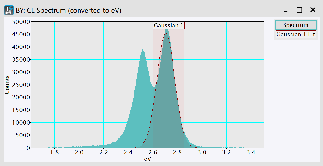
Draw a region of interest (ROI) to designate the area you want to fit.
-
With the data in the frontmost position and the Least-Square Fitting panel in NLLS mode, click the Add model button.
This will add the selected default item to the model list of the palette. The fit range will be taken from the previously made range ROI. If no such ROI is found, the range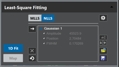 will be automatically chosen around the feature of the highest intensity (for peak models) or the center of the data (for other models).
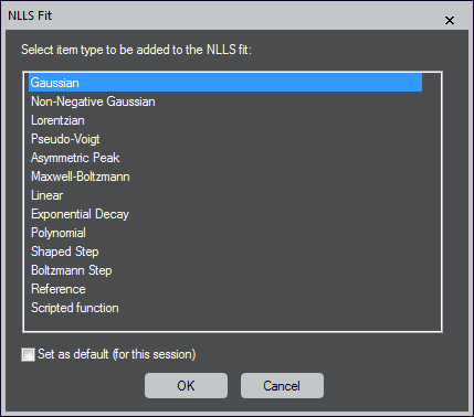
Note that you can add an item of any type by pressing the Add model button while pressing the ALT key. This will prompt a model type selection dialog to choose from. -
Adding an item to an empty list will automatically enable the live-fit. The data's line plot display will show additional slices presenting the fit results. You can customize the display in the Setup dialog. To add, you can enable or disable the live-fit manually by pressing the 1D Fit button.
-
Optional: Adjust the fitting range by resizing the range ROI labeled by the item's name. The fit will automatically recompute.
-
Optional: Resort or rename references in the list. The display will automatically update.
-
Optional: Observe the fit-parameter results by expanding the reference-entries in the model list.
-
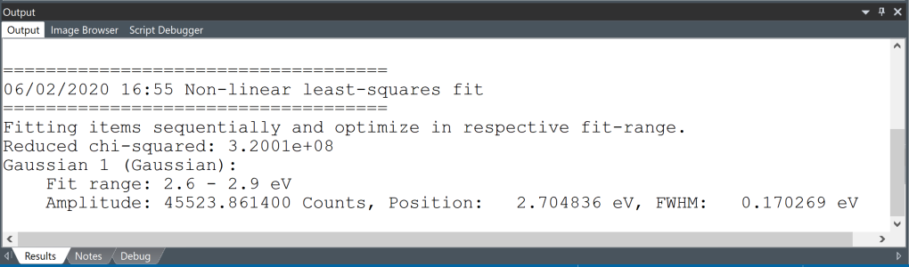
Click the 1D Fit button to output the full fit-results again while pressing the ALT key. The results will appear in the Output window.
-
Optional: Save the model setup for re-applying to different situations using the Save model button.
Spectrum Image
Non-linear least squares (NLLS) fitting involves fitting models to spectral features to quantify the spectral peak properties. Set up this fitting on the picker spectrum extracted from the spectrum image (SI) using the following workflow:
-
Select a suitable SI and bring it to the frontmost position in the workspace. Note that if the frontmost data is not suitable, the buttons in the palette will be disabled.
-
Use the spectrum picker tool to extract a spectrum from the SI and then select the spectrum.
-
Follow the steps outlined in the Single Spectrum section.
-
 Optional: Move the picker marker to investigate different areas. The live-fit will automatically recompute and adjust the fit display. This can be very useful to locate sample areas that the model does not sufficiently describe the data.
 -
Fit the references to the parent SI data by pressing the Map button.
-
Choose the fit results you want to generate. See NLLS-Fit Map Options (Output) for details.
-
Choose how to display the fit results. See NLLS-Fit Map Options (Display) for details.
-
Press OK to start the fitting procedure. The system will display the progress of the fitting routine. You can stop the fitting at any time using the Abort button.
Note: The map-fit is performed on single-position spectra, which may have significantly lower SNR than an integrated picker-spectrum. In particular, in low-intensity or high-noise data, it may be advisable to check fitting quality in the live-fit by shrinking the picker region of interest to a single pixel.
NLLS Models
 Below are the most common models that researchers use to analyze cathodoluminescence spectra.
The Least-Square Fitting tool supports multiple models for NLLS fitting that you can combine into a single fit. This section describes the various models in detail.
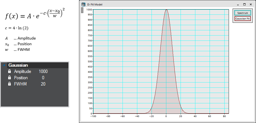
Gaussian
Peak-function characterized by a maximum position and intensity as well as the peak-width measured as the full width at half-maximum.
Non-Negative Gaussian – Limits the amplitude to positive values.
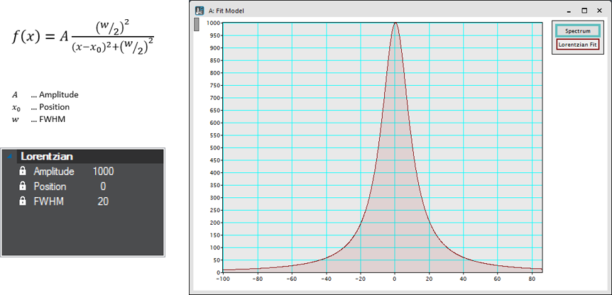
Lorentzian
Peak-function characterized by a maximum position and intensity as well as the peak- width measured as the full width at half-maximum.
NLLS Setup Palette
 Least-Square Fit Setup
NLLS Options
Fit multiple items – Choose the fit behavior when there are multiple items in the model list. This is useful for various applications since it has a profound impact on the results and different modes.
- Combined – Uses all items together as a single parameterized model that is optimized simultaneously over all specified fit-ranges
- Sequential – Fits each item on the list one after the other
The first item is fit to the original data. Each additional item is fit to the residual data of the previous fitting. The user may choose to optimize each fit over an individual or all specified fit-ranges.
- Independent – Each item is independently fit, and its parameters are optimized only over its fit-range
Defaults – Click the ... button to set the default model
Live display – Defines what options are shown as an overlay during live-fitting. These options are best explored by simultaneously observing a running live-fit.
- Total fit – Shows a slice that constitutes the sum of all references weighted by its fit coefficients
- Residual (misfit) signal – Displays a slice that represents the difference of the total fit (see above) and the actual data
- Individual fits – Presents a slice for each reference
- Colorize individually – Assigns a different color to each slice and is only available when you select the Individual fits checkbox
NLLS-Fit Map Options
After pressing the NLLS Fitting button, the map options are automatically shown at the start of a non-linear least squares (NLLS) map computation.
 Output
Fit parameter output
- Fit parameter values – Creates a map for each fit-parameter
- Show constant parameter values – When the checkbox is not selected, any fit-parameter that is locked to a fixed value will not produce a map; therefore the map would be a constant value for all pixels
Fit model output
- Total fit model – Produces an additional spectrum image (SI) data set that shows the entire fit model – The sum of all individual models
- Individual fit models – Creates additional SI data sets for each model item; the option is not available if there is only one item in the list
Additional output
- Reduced chi squared – Generates additional maps that shows the reduced chi-squared value (the root of the squared sum overall differences between model and data)
- Residual signal – Produces an additional SI data set that displays the residual signal (the difference between model and data)
Display
 The display options depend on the type of spectrum image and the number of model items in the list. For line scan data, maps become profiles.
- Show on new Workspace – Shows the mapping results on a separate workspace
- When not checked, arranges the mapping results on the largest free area of the current workspace
- Colorize maps – Colorizes the fit-parameter maps using black-to-color gradients (the same color is used either for all parameters of each model item or all parameters of the same name)
 Add map labels – Adds label annotations to all maps – Use the color-picker button to specify the color of the annotation
- Add intensity scale – Includes an intensity scale annotation on all maps
- Stack profiles – For line scan data, maps become profiles
When this option is checked, it compiles all profile data into a single line-plot display that shows multiple slices. Either all parameters of each model item or the same name are stacked into a single display.
Tips and Tricks
Analyzing luminescence spectra
Researchers use many luminescence techniques as a qualitative, exploratory tool and to frequently analyze data variations from different laboratories. However, it is essential to distinguish between differences that arise from sample variations or treatments versus signal collection and processing artifacts. Below are steps we recommend following when analyzing and reporting spectral data.
-
Perform measurements under known scanning electron microscope conditions, e.g., electron dose and power density.
-
Collect the raw data (in wavelength, I(λ)dλ versus λ) and verify the data is repeatable.
-
Process the data.
-
Removal of dark current (if any).
-
Correct for any non-linearities in the efficiency of the detection system.
-
Convert spectra from dispersive units of wavelength (nm) to energy (eV).
-
Use linear least-squares fitting to deconvolve spectral features.
-
-
Publish the data and ensure to include the factors above.
Unfortunately, not all researchers follow these steps and a range of systematic errors make their way into the published literature. The following section aims to explain why each step is important and the potential issues you may encounter.
Power density
It is important to characterize the power density in many specimens since most luminescence processes exhibit a strong variation in the intensity of cathodoluminescence (CL) emission with electron beam current, size of interaction volume, and scanning area. Failure to investigate or account for this effect can lead to drawing incorrect conclusions. However, this effect is useful to investigate the nature of a luminescence signal and reveal details of the recombination mechanism by plotting the CL intensity versus power density.
The power density versus emission intensity can be written as follows:\(Intensity_{CL} ∝Dose^m\)
Plotting the intensity versus dose relationship using \(log[Intensity_{CL}]∝m.log[Dose]\) allows m to be determined.
When m ≤ 1, the mechanism is via deep levels (impurities) or free-bound and donor-acceptor pairs; when m ≥ 1, corresponds to near band edge emission and for excitonic processes, 1 ≥ m ≤ 2 with m = 1 for free exciton and m = 1.5 for bound excitons.
Increasing electron dose (power density) can also lead to a peak shift in materials that exhibit a piezoelectric field, e.g., nitride semiconductors with the wurtzite crystal structure.
Verify the data is repeatable
It is often assumed that capturing luminescence signal(s) is a passive process, and indeed in some cases, this is correct. However, the act of sample stimulation by an electron beam can modify the intensity and emission spectra. For example, radiation damage may occur to the sample and track with changes to the electron microscope's beam exposure. Several noticeable examples include:
- Quenching of emission from covalently bonded molecules
- Creation of new point defects when using electrons with energies greater than the knock-on damage threshold—particularly important in the analysis of semiconductors in the TEM
- Rearrangements into new defect complexes and/or charges that are transferred between sites
These effects can modify the intensity, spectrum, and associated excited-state lifetimes of the processes. Therefore, it is prudent to minimize the electron dose and acquire the spectra with minimal beam-induced effects. When studying new materials, it is often a valuable exercise to investigate these effects before drawing any conclusions.
Luminescence spectroscopy also offers insight into these dynamic processes and techniques may include simultaneous excitation methods to follow transient events.
Process the data
Typically, a raw spectrum is captured and plotted as a 1D plot displaying intensity versus wavelength. However, accurate analysis and processing of the data require several steps and careful consideration of any system contributions to the data.
Removal of the dark current
Most luminescence detectors (e.g., CCDs and photomultiplier tubes (PMTs)) exhibit a dark current that needs to be removed to prevent errors in subsequent processing. The dark current is a relatively small electric current that flows through photosensitive devices even when no photons are entering the device. Dark (frame) subtraction can remove an estimate of the mean fixed pattern, but sometimes this must be performed as a post-processing step.
Correct for change(s) in the detection system
A wide range of detection systems are available to measure luminescence spectra, including commercially supplied detectors and home-built setups. In both cases, these detectors may incorporate a wide range of elements, including the optical components (mirrors, lenses, spectrometers) and detectors (PMTs and cameras). The performance (reflectivity, transmission, or sensitivity) of individual components will vary by wavelength (and polarization). These components may be combined within a system to deliver a unique response by wavelength (and polarization) that can vary by several orders of magnitude across the wavelength range. This correction may be essential when trying to compare a measured spectrum to the literature or compare the intensity ratio of peaks in a spectrum. Be mindful that the literature does not always make it clear whether raw or corrected data is being presented.
With modern equipment, it is often possible to correct for the system response. Within Gatan Microscopy Suite® software, right-click the mouse on a CL spectrum to access this correction.
Below are key components of a standard luminescence system and where you typically observe significant changes in performance:
Focusing optics
Many detection systems utilize focusing optics to couple the collected light into the spectrograph. However, the transmission lenses or mirror reflection efficiencies can vary significantly with wavelength. For example, many mirror components use protected aluminum that has a reflectivity of ~96% at visible wavelengths but falls to <70% at 200 nm. In transmission lenses, one must also consider the effect of chromatic aberration—the change in focal length of an optical component by wavelength—which can reduce the light coupling efficiency by a factor of >1000 compared to visible wavelengths.
Diffraction gratings
Diffraction gratings form the dispersive element of a spectrometer or spectrograph, producing a signal on a linear wavelength axis. The ruling density (also known as groove- or line-density) determines the dispersion (different levels of spectral resolution) and the blaze wavelength (λBlaze); the wavelength at which it operates most efficiently. The response efficiency usually falls to less than 10 – 20% of the peak value by ∼½λBlaze and ∼2λBlaze; this defines the useful spectral range of the grating. Careful selection of the appropriate diffraction grating blaze for a given experiment is needed and, when covering a significant wavelength range, the change in response must be considered.
Diffraction gratings also exhibit higher-order diffraction (dsinq = nλ where q is the diffraction angle and n an integer). When a spectrum covers a wide spectral range, you may observe second-order peaks unless order sorting blocking filters are used. For example, you may use a grating blazed at 300 nm to capture a spectrum spanning 200 – 700 nm, and, at a wavelength setting of the spectrometer of 600 nm one will also detect the second-order light of 300 nm, and the third-order light of 200 nm.
Detectors
A CL system may employ several types of detectors, including PMTs, photodiodes, cameras (CCD or CMOS), and linear diode array. You can record a change in sensitivity across the wavelength range that each detector type exhibits during a CL experiment. For instance, when you use a scientific-grade camera with a nominal operating range from 200 – 1100 nm, the efficiency fluctuates by almost two orders of magnitude over that range. There also exists a significant variation within each type of detector and it may change with age. These limitations must be recognized.
We recommend that published data clearly states whether the correction for the total system response is applied. However, please note that publications do not always include this information.
In contrast, it is not necessary to apply this correction during some experiments, e.g., when performing initial analyses or when analyzing a very limited wavelength range. However, for peaks with a broad full width at half maximum, this becomes almost essential as the system response often leads to an apparent change between the peak position in raw and corrected data.
Convert spectra from dispersive units of wavelength (nm) to energy (eV)
The intrinsic shapes of luminescence emission bands are symmetrical peaks (often Lorentzian- or Gaussian-shaped) when displayed in energy (E, eV) as the unit of dispersion. This shape is due to the broadening of the electronic energy levels which drive the electron transitions that generate photon emissions. Most hardware for luminescence spectrum acquisition, record the data dispersed by wavelength (λ, nm) using a fixed wavelength bandwidth (dλ), e.g., a spectrum is plotted as (I(λ)dλ versus λ). However, due to the inverse relationship of energy and wavelength, dλ versus dE is not a constant and therefore, spectral features displayed in wavelength as the dispersive units are not symmetrical. This leads to several possible issues:
- Deconvolution using the non-linear least squares (NLLS) fitting has no physical meaning in spectra with wavelength as the units of dispersion
- An apparent difference in peak positions of wavelength and energy data
- When a spectrum consists of more than one spectral feature, the relative intensity of the peaks will alter
The reason for these difficulties is that in the transformation from wavelength(λ) signals (I(λ)dλ versus λ) into the energy plot (I(E)dE versus E) the transformation of the wavelength axis into terms of energy is obvious (i.e. using \(E ∝ hc/λ\)). However, for the intensity axis, the transformation requires an intensity correction from wavelength to the energy of (I(E) dE) and a change from the fixed wavelength bandwidth to a fixed energy bandwidth, related by dE = -hc/λ2dλ. Particularly for broader luminescence features, the (1/λ2) term has a major distortion effect on the curve shapes.
Deconvolve spectral features
Please refer to NLLS Models section.
Spectral calibration
The central wavelength of a peak in a spectrum is often reported with high precision (two decimal places or more), but the error in this measurement is rarely stated. In many systems with a manual grating selection, the accuracy of spectral calibration may be as much as ±0.2 nm and the precision ±2 nm unless a spectral calibration is performed immediately before measurement.
Thus, take care when comparing measured to data to that in the literature. Fortunately, in many CL experiments that occur at room temperature, it is often the wavelength shift that is important rather than the accuracy of a single measurement.
Summary
The section highlights the need to process luminescence spectra in a meaningful way, make accurate calibrations, and to recognize that this is done to varying degrees in the literature. This is true for all luminescence methods regardless of the excitation source. The intention here is to provide sufficient information that a researcher may understand which methods are important when drawing conclusions from an experimental result.